Yeah, in geek speak it's a PCB which stands for Printed Circuit Board. It's the green board you see when you open up your tv or computer. We have to make a few to get Libramentum up and running, and they have to be done by Tuesday. Let me take you through the process.
When we choose the components we want, like which processors and which accelerometers, they come with a data sheet that detail everything you need to know to get the thing running and how to extract the information. It'll tell you things like the maximum and minimum voltage levels, maximum current draw and where to put all the little resistors and capacitors that you see around a microchip. With this information we can get to work and start making electrical schematics to show how the electrons are going to make it from chip to chip. Schematics: Completed.
We're now coming to the end of the hard part. This is where we look up every single individual component and order it, as well as recording the details of the size and shape so that we know where to put the holes and the solder pads on the PCB. We save this information against each component on the schematic. It's not hard - until you can't find a source for the part you want, or the dimensions are not already in the library of 'footprints' and we have to make them up ourselves. This won't make any sense to anyone who isn't into this sort of geeky stuff, but I'll come back later and load some pictures to show you what I mean.
Once we have a footprint loaded against each component on the scematic we can run a program which places each footprint on a digital PCB. Then we can simply click and drag to get them all fitting on the outline and try to place them so that the solder tracks won't have to cross each other. From there we can run the "Auto-route" and the computer will try to connect all the pins up itself. If there are contentions, then that's for us to sort out and that's the hard part. My lab partner and I have been working on these PCBs for several weeks now and we're starting to get really sick of it!
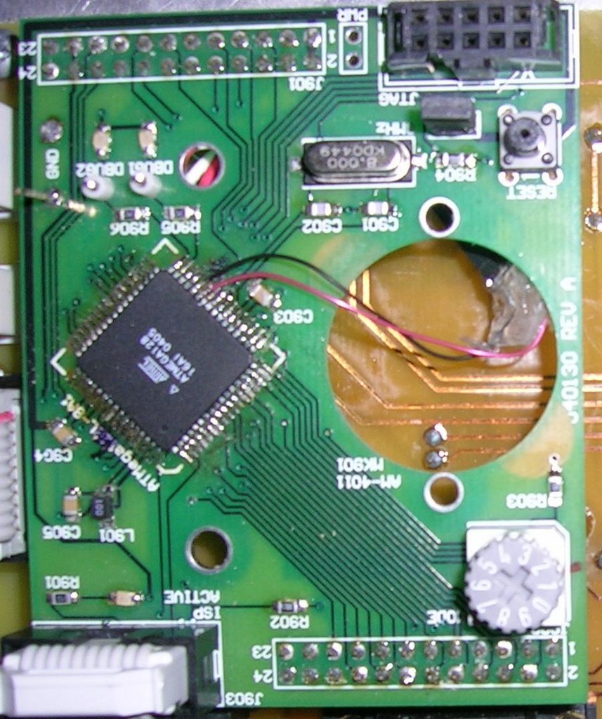
Okay, here's a breakdown with images of the design process. I'll use images from the power supply so as not to compromise our intellectual copyright (as it were).
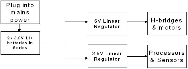 This is the basic outline of what we want to achieve. See how we have seperated the motor supply from the proccessors. This is because the motors can introduce noise which is in the form of voltage and current spikes. These spikes can seriously damage the more delicate processors. Next we need to take these components - the voltage regulators and the charging micro chips and turn our design concept into a schematic diagram.
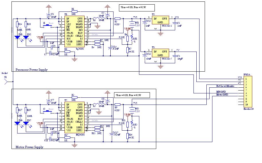 The two big yellow components are the charging micro chips. You can see they have a lot of inputs and outputs to make sure they won't blow up the batteries. There are two lots of two batteries, one set each charged seperately. Then on the right are some small yellow voltage regulators for 3.2V and 5V. The 6V system for the motors didn't need to be regualted in the end. So now all those little resistors and capacitors, inductors, diodes and microchips need to be 'placed' on an electrical design of the PCB, here's an image of what a 'footprint' for a microchip might look like;
 This particular footprint is designed for a 'quad flat package' micro chip which has 32 pins. The green rectangles will become solder pads on the PCB and the red lines are just guide marks. This particular chip is only a few milimetres across so you can imagine how tiny those solder pads are, and the hassle it would be if we got our dimensions even a little bit out!
So now you can see what I have been talking about when I say we had to find or design the correct footprint for every single component on the shematic. The computer will transfer those footprints onto the digital PCB and try to put lines that represent solder tracks between all the pins, but it can get very complicated and in the end we
had to opt for double sided boards. This means we can have solder tracks crossing each other by travelling onto the other side of the PCB first. It is much more complicated to manufacture a double sided board and in the end we may even have to go to a company who will do it for us. Here's a glimpse at what the finished design for the power supply PCB will look like:
 It doesn't make much sense does it? Well in the end it doesn't have to. This very image will be printed out onto basic transparent OHP plastic and placed on top of the blankboard. The board has a layer of conductive material across it. During the manufcturing process the board is bombarded with UV light except for the areas where the ink from the printed desgn halts the light. Then the plastic design is removed and the board is placed in an acid bath. The weakened metal will be eaten away and the protected metal remains, and there you have your tracks and pads, ready for soldering. Easy!
Hopefully the finished product will look something like this design:

8 comments:
A note to browsers - the above links are apparently to New York City Street Fairs, and thus have nothing to do with robots or programming. However I in no way discourage you to have a look if you're interested.
Here are some links that I believe will be interested
Your are Excellent. And so is your site! Keep up the good work. Bookmarked.
»
Hey what a great site keep up the work its excellent.
»
Coll now 09452588392 friends join kero play boy sex job koi dhoka dhari nahi join kero or money kamaya jo mel female hii profile ke madem callege girl house wife ki sath home service hotel service join kero or money kamaya jo mel female hii profile ke madem callege girl house wife ki sath home service gigolo job all India ke all city mi service available college girl house wife anti ki key i service available call new 09452588392 full Maza masti key Saath psaa kamye all ki all city's mey available service gigolo coll boy play boy serwis all India ki all city's mey available service gigolo coll boy play boy serwis all India ki all city's mey available service gigolo coll boy play boy serwis all India ki all city's mey available service gigolo coll boy play boy serwis all India ki all city's mey available service gigolo coll boy play boy serwis all India ki all city's mey available service gigolo coll boy play boy serwis all India ki all city's mey available service gigolo coll boy play boy serwis all India ki all city's mey available service gigolo coll boy play boy serwis all India ki all city's mey available service gigolo coll boy play boy serwis all India ki all city's mey available service gigolo coll boy play boy serwis all India ki all city's mey available service gigolo coll full Maza masti key Saath psaa kamye all India ki all city's mey available service gigolo coll boy play boy serwis all India ki all city's mey available service gigolo coll boy play boy serwis all India ki all city's mey available service gigolo coll boy play boy serwis all India ki all city's mey available service gigolo coll boy play boy serwis all India ki all city's mey available service gigolo coll boy play boy serwis all India ki all city's mey available service gigolo coll boy play boy serwis all India ki all city's mey available service gigolo coll boy play boy serwis all India ki all city's mey available service gigolo coll boy play boy serwis all India ki all city's mey available service gigolo coll boy play boy serwis all India ki all city's mey available service gigolo coll boy play boy serwis all India ki all city's mey available service gigolo coll boy play boy serwis all the time coll me know when you are in the time coll now 09452588392 koi dhokha dhadhi nhi full secret service providers all India ki all city's mey available service gigolo coll boy play boy serwis all India ki all city's mey available service gigolo coll boy play boy serwis all India ki all city's mey available service gigolo coll boy play boy serwis all India ki all city's mey available service gigolo coll boy play boy serwis all India ki all city's mey available service gigolo coll boy play boy serwis all India ki all city's mey available service gigolo coll boy play boy serwis all India ki all city's mey available service gigolo coll boy play boy serwis all India ki all city's mey available service gigolo coll boy play boy service gigolo coll boy play boy service gigolo coll boy play boy serwis all India ki all city's mey available service gigolo coll boy play boy serwis all India ki all city's mey available service gigolo coll boy play boy serwis all India ki all city's mey available service gigolo coll boy play boy serwis all India ki all city's mey available service gigolo coll boy play boy serwis all India ki all city's mey available service gigolo coll now 09452588392 SECRET 💯%
CALL NOW
A cybersecurity official from the Ministry of Public Security told Xinhua that the internet ID service was strictly “voluntary,” but the government encourages various industries and sectors to integrate with it.
성남출장샵
남원출장샵
영주애인대행
애인대행
애인대행
CALL NOW
Post a Comment